Days in semi.ac - 1
在半导体所的经历 - 1
Institute of Semiconductors Chinese Academy of Sciences, which is known as semi.ac, is the major research facility of the frontier technology of the semiconductor industry and science in China. I’ve been in the semi.ac since last summer in 2015. After a year of studying and practicing, I didn’t achieved much in the research group. But I really gained some valuable experience in this period of time.
Tours and conferences
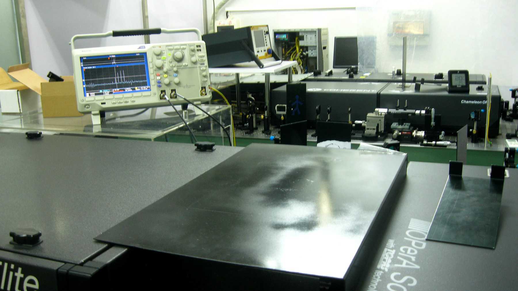
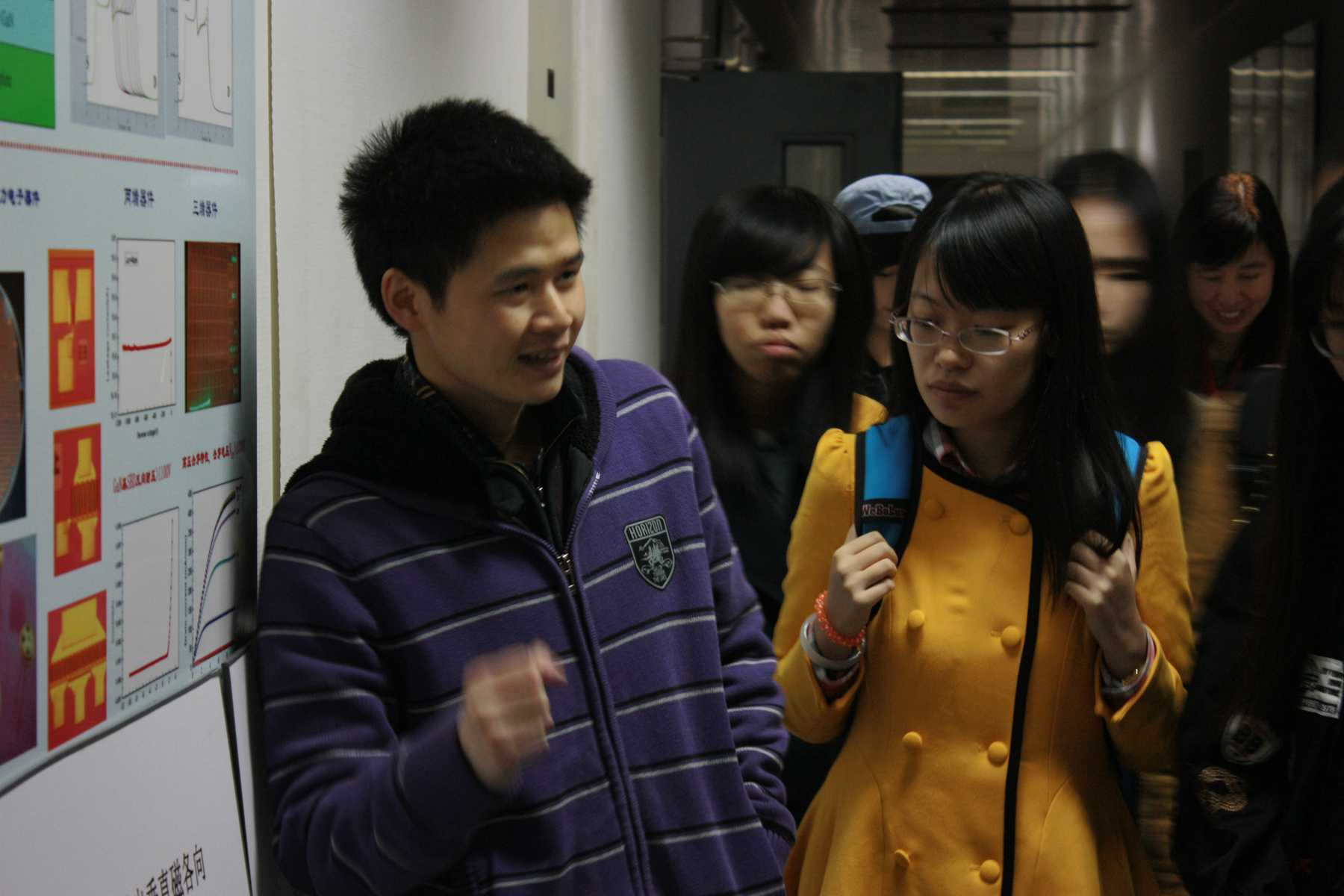
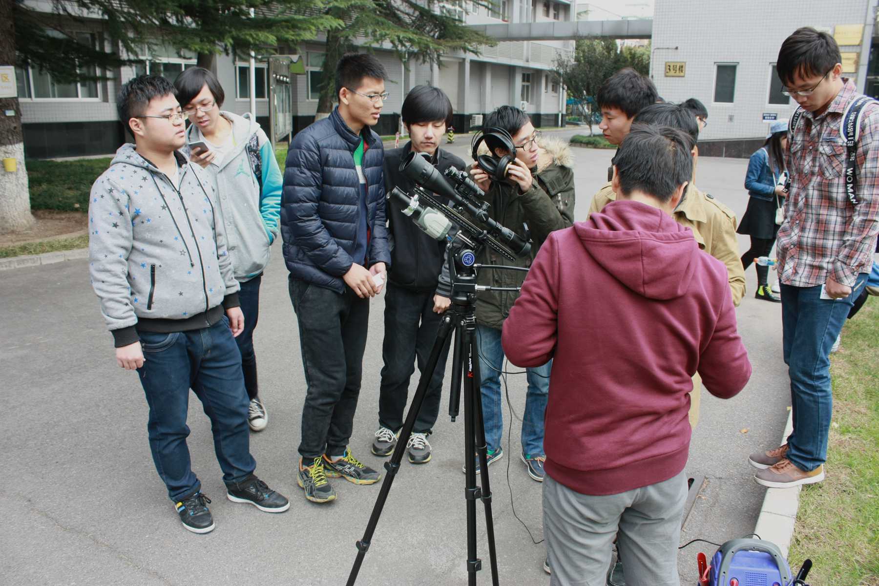
The first time I went to the institute was in May, 2015. The students and professors there gave our undergraduates a concise introduction about the fields of their researches, including nano-electronics, femtosecond-laser devices, nano-structures and microwave photons, bio-electro, semiconductor and diodes and some other things.
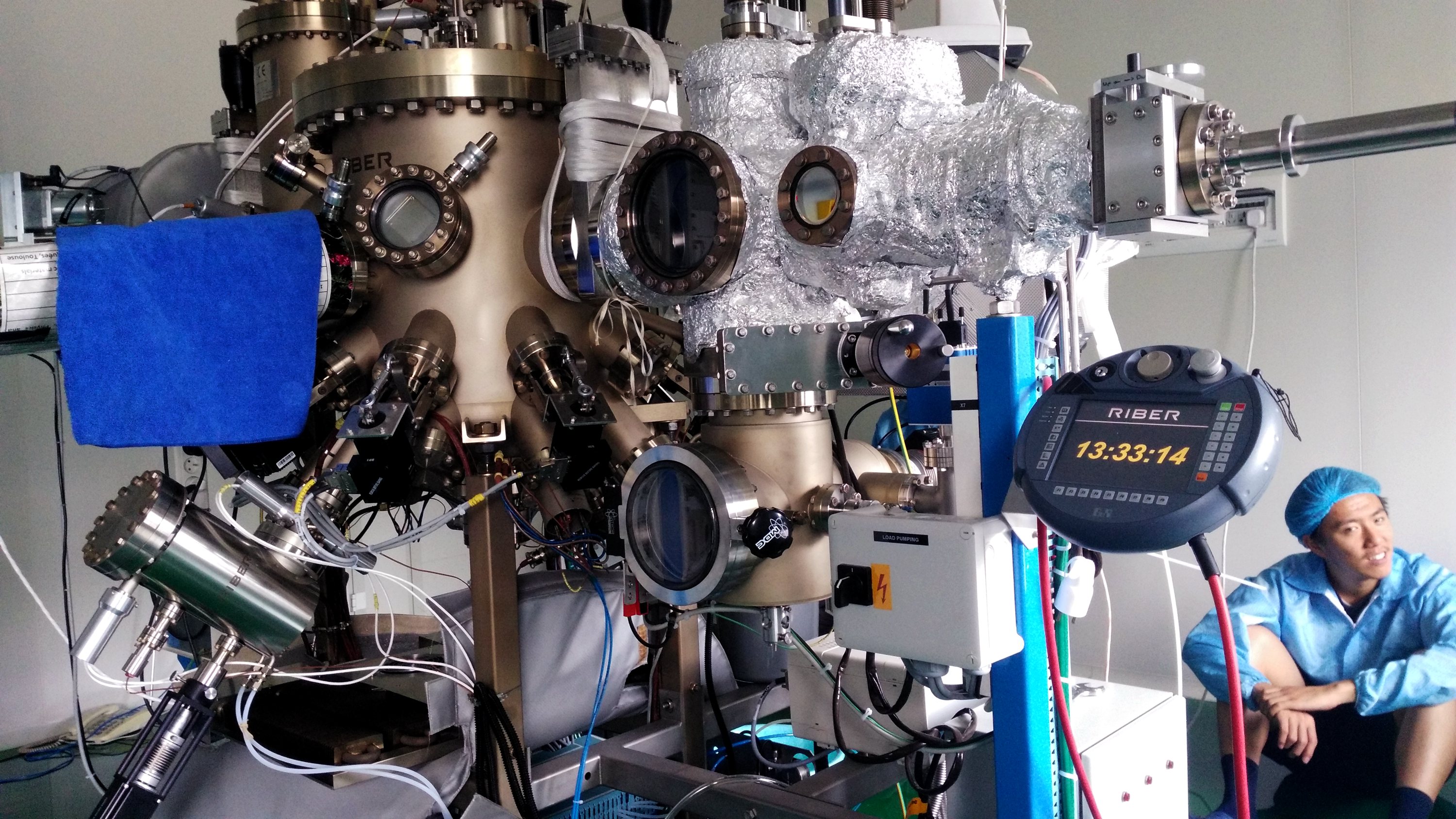
It’s pretty a brand new impression to me as I see all this tubes wandering about in the facility, filled with liquid nitrogen. There are also some really hug device such as the MOCVD and MBE and Photoluminescence Spectroscopy device.
In autumn, we went there for a meeting.
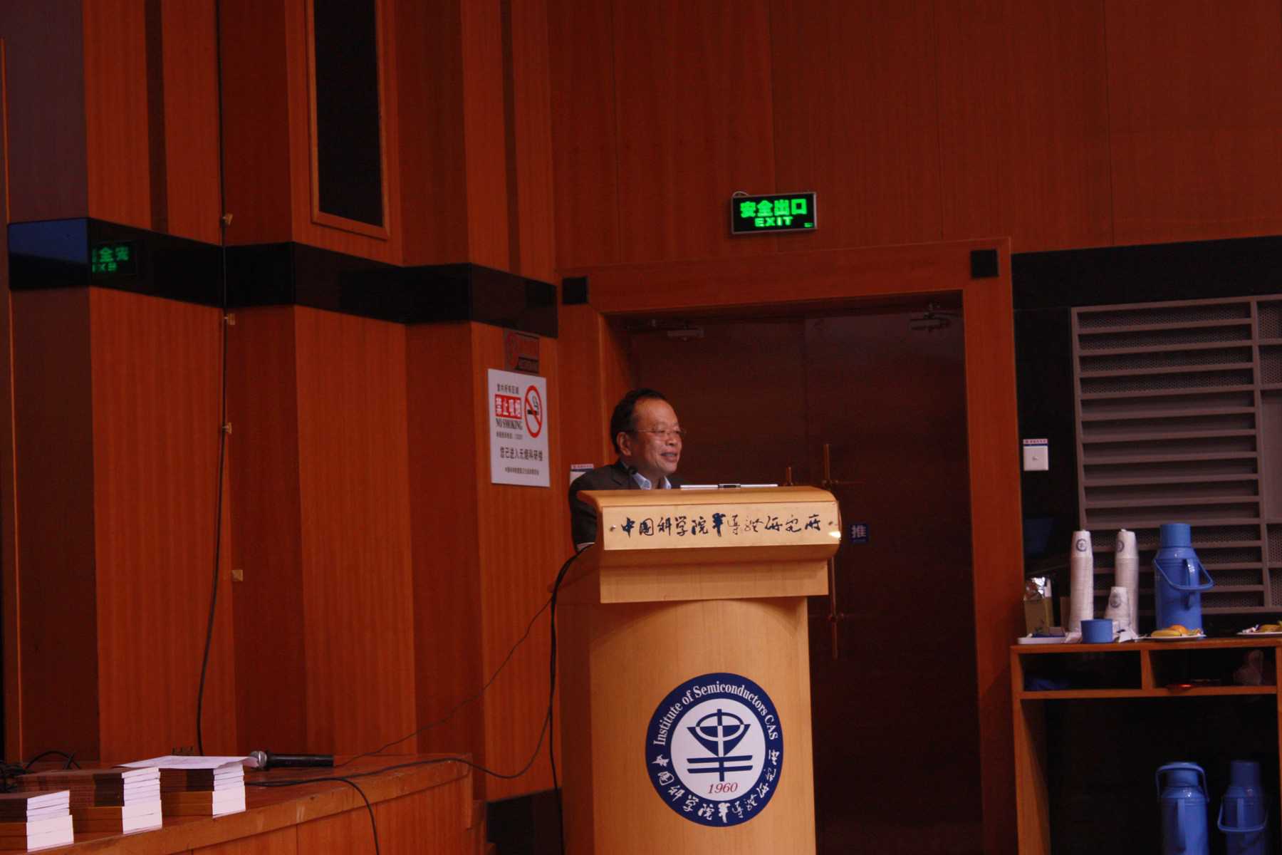
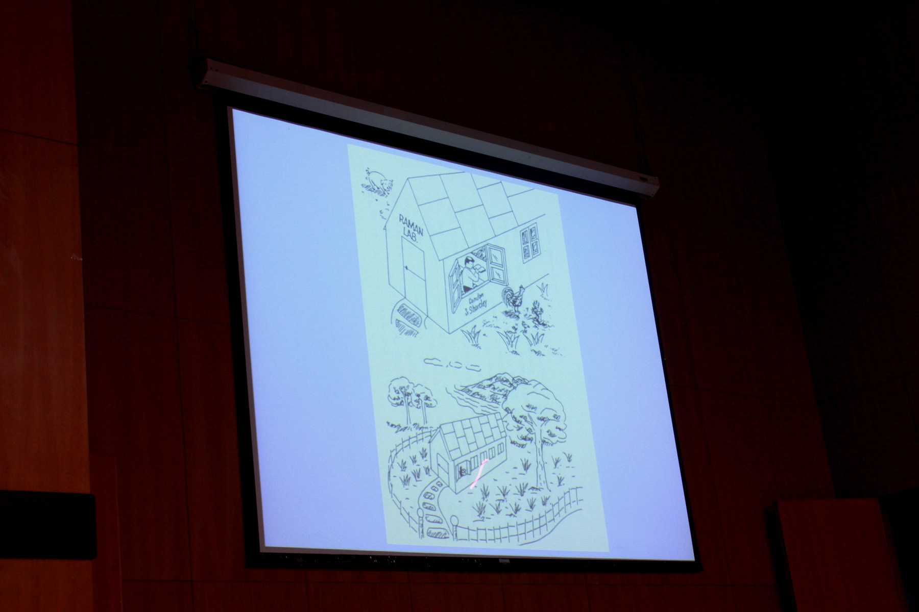
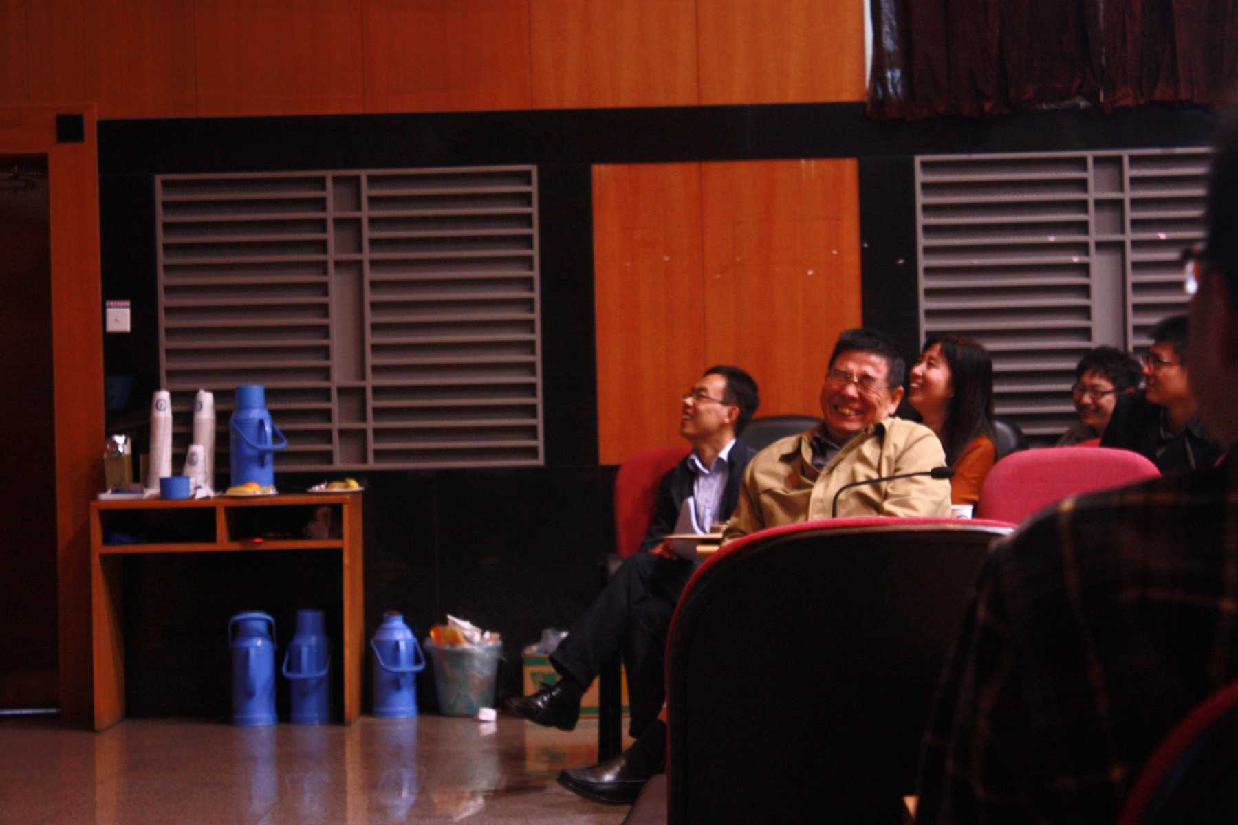
The academician’s report introduced the biography of Huang Kun, the founder or Huang’s equation and the industry of solid state physics in China. A cartoon which depicts the life of Huang at Raman Lab vividly showed the hardship and incovenience at that time: he had to raise pigs and chicken while dealing with his research works ! After seeing this picture, all the students and teachers smirked with joy. The director even get so excited as the photo above…
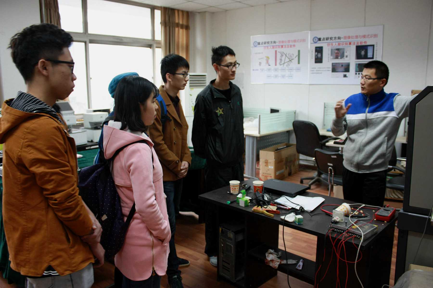
The other day we tour some labs. One of them deal with the Visible Light Communication issue. It happened that I was doing some research on that topic then, and I got a lot of inspiration from them. We maintained solid connection for about half a year and I finished up with a prototype VLC device with the help of them.
The other lab mainly focus on the nano-material subject and we got closed enough to observe the operation of a MBE.
Experience and studies
从去年夏天到2016年2月左右,基本去半导体所基本就是参观和简略了解内容。然而,始终没有实际进行研究不能让我们得到更多的提升。因而,我和另外三个同学先是参与了有关三五族材料制备染料敏化太阳能电池和研究的工作,包括微纳加工等等的内容。之后又独自参与了有关光学微腔的研究。
Currently, I’m doing some research on the topic of microcavity and whispering gallery mode optical device. Did some simulation and analysis. You may want to check it out in my album and other blogposts
Related Post: Days in semi.ac - 2

Leave a Comment